


 02 9541 3500
Why You Need an Electron Microscope in Additive Manufacturing
Additive manufacturing (AM) is a technology that uses three-dimensional computer models to print parts by building the component layer-by-layer. Construction, prototyping and biomechanical are some popular applications, but opportunities exist anywhere minimal raw materials requirements and a greater design freedom are desired. In this article, we explore the advantages of using a Scanning Electron Microscope for AM, common use cases and how the Phenom XL G2 Desktop SEM can also determine the elemental composition for every identified particle.
What is SEM, and What Does an SEM Image Tell You?
Scanning Electron Microscopy (SEM) provides microscopic information about the surface or near-surface region of a sample. The only requirement is that the viewed object must have the capability to withstand the vacuum within the chamber and the bombardment of the electrons.
SEM enables examining the interaction between electrons generated by the source at the top of the column, accelerated toward the sample, and the atoms that make up the sample. These electrons interact with the sample’s surface to produce signals collected by the detector that provides an image or chemical composition. The interaction of the electrons from the source beam generates different signals and a drop-like interaction volume within the sample, typically generating Secondary Electrons (SE) within the first 10nm of the sample’s surface. As electrons go deeper, Back Scatter Electrons (BSE) emerge from the sample, and if electrons have enough energy, they can generate X-rays.
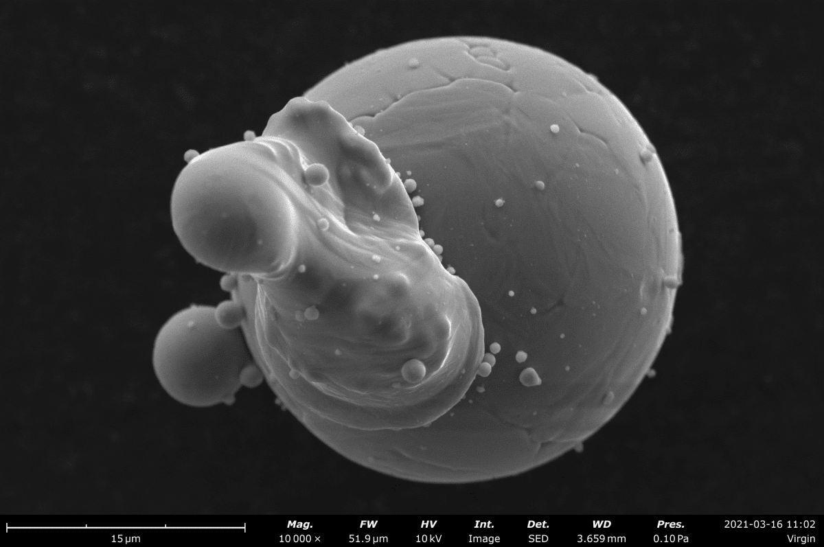
Dark and bright areas characterise SE images, and their contrast gives a sense of depth and dimensionality. Examiners use SE images to analyse the morphology of a sample. The advantage of a SED is that it provides information about the surface topography, clearly displaying any bumps and dips on the surface. BSE images provide information about element distribution, with the darker areas indicating low density or light material such as carbon. In comparison, the brighter regions indicate heavier elements such as copper and zinc. BSE images are therefore helpful in identifying contaminants on the surface of the sample.
Elemental Analysis for Additive Manufacturing
Energy Dispersive Spectrometry (EDS), or Energy Dispersive X-ray (EDX) microanalysis, is a non-destructive analytical technique that determines sample composition using X-rays generated from the interaction of electrons from the source with the sample. The working principle involves electrons from the beam crossing through an atom, which forces the ejection of an electron. Another electron from higher energy fills the vacancy and leads to an X-ray emitted, which is characteristic of the element of that atom.
Uses of SEM in Additive Manufacturing
Typical 3D printed parts require accurate quality control to identify any faults or contaminants in the material that may compromise the reliability of the part. Using SEM, one can inspect printed parts for cracks or inclusions, print resolution, and the presence of different phases, characterise particles for their morphology and composition, or validate raw materials or recycled materials. BSE imaging can reveal different stages in components as these phases have different densities. Using BSE imaging, a cross-section of an element can show the distribution of different phases or densities in components usually formed in processes that involve fluctuating, high temperatures. Both BSE and SED detectors can provide images of the sample surface and show pores, cracks, and inclusions. In contrast, the EDS detector provides the elemental composition to provide valuable fracture or metal wear analysis. The recycling process can change the original size and shape of the powder and form agglomerates, which can form pores within the sample and result in lower-quality printing.
SEM can therefore provide a great deal of information to improve the quality of the final product. SEM is a versatile tool that can give quick verification and classification of materials. SEM images provide structural information and chemical composition in addition to particle morphology and the presence of aggregates. Uniform shape, size, and elemental distribution of the powder samples used for AM are crucial to creating high-quality 3D printed structures.
Particles are identified and measured using automated software that extracts and reports statistical distributions of characteristic geometrical properties. This software also sorts and classifies individual particles during runs based upon particle size or particle chemistry. Identification of particles that fall outside the set criteria for each classification enables grouping and capturing and reporting of extensive information. SEM can count every particle in a given population field, so particle size distribution is displayed as a number distribution histogram. The elemental composition identifies and separates them by particle size.
The most significant advantage of using an SEM for AM is determining the chemical composition for every identified particle. The other noteworthy advantage is the ability to understand particle shape and particle size distribution by number. This individual particle analysis helps to highlight the presence of fine or minuscule particles that can create problems in terms of flowability in the printing process. As particles get smaller, the forces of attraction between particles increase, which means finer powders are usually less free-flowing than coarser powders. Smooth, regular-shaped particles tend to flow more easily than rough-shaped ones because of reduced friction and interlocking.
Identify Failures and Root Cause Faster with the Phenom ParticleX SEM
The Phenom ParticleX package for AM provides 3D printing companies faster quality control analyses of materials. The Phenom’s compact size requires very little space and allows users to place the microscope exactly where it’s needed. Whether that’s in the lab or on the production line, Phenom ParticleX offers in-house analysis and validation of produced goods against industry-approved standards, up to ten times faster than outsourcing.
Consisting of a high-performance Phenom XL G2 Desktop SEM and a broad range of automated SEM analyses, the system pairs SEM microscopy with energy-dispersive X-ray (EDS) spectroscopy. This powerful combination provides structural details and chemical composition to enable greater insight when assessing the quality of a product. Users can obtain high-quality images in just 40 seconds—three times faster than other desktop SEM systems on the market. The system enables more resolving power, with an improved resolution of 10 nanometers and exploring large samples of up to 100 by 100 millimetres. The secondary electron detector (SED) is ideal when studying microstructures, fibres, or particles to reveal detailed sample surface information. Users can see what elements are present with the elemental mapping and line scan functionality using live energy-dispersive X-ray (EDS) analysis with a click on the impurity.
ParticleX software quantifies powder morphologies, size distribution, homogeneity, and contaminants in an automated fashion to evaluate the purity of metal particles at the microscale. This visibility helps to optimise recipes and assists with the recycling of raw materials by measuring various size and shape parameters, such as minimum and maximum diameter, perimeter, aspect ratio, roughness, and Feret’s diameter. All of these can be displayed with 10%, 50%, 90% values (e.g., d10, d50, d90).
The Phenom SEM package for Additive Manufacturing is designed to provide 3D printing companies faster quality control analyses of materials. Contact us for a demonstration or quote today!