


 02 9541 3500
The Applications and Practical Uses of Scanning Electron Microscopes
Scanning Electron Microscopes (SEMs) are used across a number of industrial, commercial, and research applications. From cutting edge fabrication processes to forensic applications, there’s a diverse range of practical applications for the modern SEM.
How SEMs work
A Scanning Electron Microscope (SEM) uses focused beams of electrons to render high resolution, three-dimensional images. These images provide information on:
- topography
- morphology
- composition
A schematic representation of an SEM is shown in Figure 1. Electrons are generated at the top of the column by the electron source. They are then accelerated down the column that is under vacuum, which helps to prevent any atoms and molecules present in the column from interacting with the electron beam and ensures good quality imaging.
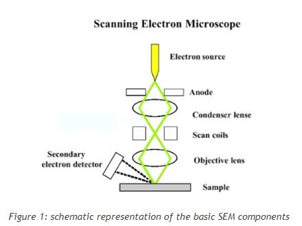
Electromagnetic lenses are used to control the path of the electrons. The condenser defines the size of the electron beam (which defines the resolution), while the objective lens’ main role is the focusing of the beam onto the sample. Scanning coils are used to raster the beam onto the sample. In many cases, apertures are combined with the lenses in order to control the size of the beam.
Different types of electrons are emitted from samples upon interacting with the electron beam. A BackScattered Electron (BSE) detector is placed above the sample to help detect backscattered electrons. Images show contrast information between areas with different chemical compositions as heavier elements (high atomic number) will appear brighter. A Secondary Electron (SE) detector is placed at the side of the electron chamber, at an angle, in order to increase the efficiency of detecting secondary electrons which can provide more detailed surface information.
How is electron microscopy different to optical microscopy?
The key difference between electron and optical microscopy is right there in the name. SEMs use a beam of electrons rather than a beam of light. An electron source located at the top of the microscope emits a beam of highly concentrated electrons.
In SEMs, there are three different types of electron sources:
- Thermionic filament – A Tungsten filament inside the microscope is heated until it emits electrons. A Tungsten filament operates at white-hot temperatures which means it gradually evaporates with time and eventually breaks which can contaminate the upper part of the electron column. The average lifetime of a Tungsten source is about 100 hours, depending on the vacuum.
- Field emission gun (FEG) – Generate a strong electrical field that pulls electrons away from their atoms. This is typically the more popular choice in SEMs as it generates high resolution images, however it requires a vacuum design that often comes at a high price.
- Cerium Hexaboride cathode (CeB6) – provides ten times the brightness compared to Tungsten which means a better signal-to-noise ratio and better resolution. A CeB6 source typically provides more than fifteen times the service life of Tungsten: 1500+ hours. A CeB6 source is used in all the desktop Phenom SEM series of instruments.
Applications of SEMs
SEMs can be used in a variety of industrial, commercial, and research applications.
Materials science
SEMs are used in materials science for research, quality control and failure analysis.
In modern materials science, investigations into nanotubes and nanofibres, high temperature superconductors, mesoporous architectures and alloy strength, all rely heavily on the use of SEMs for research and investigation.
In fact, just about any material science industry, from aerospace and chemistry to electronics and energy usage, have only been made possible with the help of SEMs.
Nanowires for gas sensing
Researchers are exploring new ways nanowires can be used as gas sensors by improving existing fabrication methods and developing new ones. Electron microscopy is vitally important in helping characterise nanowires and understanding their gas sensing behaviour.
Semiconductor inspection
Reliable performance of semiconductors requires accurate topographical information. The high resolution three dimensional images produced by SEMs offers a speedy, accurate measurement of the composition of the semiconductor.
In fact, in just about all wafer manufacturing processes, SEMs are one of three essential quality control tools used. In the case of repetitive daily quality control tests, larger monitors (19 inches) have been shown to reduce visual fatigue for inspectors.
Microchip assembly
Microchip production is increasingly relying on SEMs to help gain insight into the effectiveness of new production and fabrication methods. With smaller and smaller scales and materials, as well as the potential of complex self assembling polymers, the high resolution, three-dimensional capacity of SEMs is invaluable to microchip design and production.
As the Internet of Things (IoT) becomes more prevalent in the day to day lives of consumers and manufacturers, SEMs will continue to play an important role in the design of low cost, low power chipsets for non-traditional computers and networked devices.
Forensic investigations
Criminal and other forensic investigations utilise SEMs to uncover evidence and gain further forensic insight. Uses include:
- analysis of gunshot residue
- jewellery examination
- bullet marking comparison
- handwriting and print analysis
- examination of banknote authenticity.
- paint particle and fibre analysis
- filament bulb analysis in traffic incidents
Since SEMs offer the ability to examine a wide range of materials at high and low magnification without sacrificing depth of focus, their use in forensic sciences makes it possible to draw conclusions, identify material origins and contribute to a body of evidence in criminal and legal matters. The desktop Phenom GSR instrument is specifically designed for automated gun shot residue analysis.
Biological sciences
In biological sciences, SEMs can be used on anything from insects and animal tissue to bacteria and viruses. Uses include:
- measuring the effect of climate change of species.
- identifying new bacteria and virulent strains
- vaccination testing
- uncovering new species
- work within the field of genetics
Soil and rock sampling
Geological sampling using a scanning electron microscope can determine weathering processes and morphology of the samples. Backscattered electron imaging can be used to identify compositional differences, while composition of elements can be provided by microanalysis. Valid uses include:
- identification of tools and early human artefacts
- soil quality measurement for farming and agriculture
- dating historic ruins
- forensic evidence is soil quality, toxins etc.
Medical science
Broadly speaking, SEMs are used in medical science to compare blood and tissue samples in determining the cause of illness and measuring the effects of treatments on patients (while contributing to the design of new treatments). Common uses include:
- identifying diseases and viruses
- testing new vaccinations and medicines
- comparing tissue samples between patients in a control and test group
- testing samples over the lifespan of a patient
Art
Not all SEM applications are strictly practical. Micrographs produced by SEMs have been used to create digital artworks. High resolution three dimensional images of various materials create a range of diverse landscapes, image subjects are both alien and familiar.
A practical and useful tool
Within the fields of industrial application and research, there is an increasing focus on quality control at microscopic scales. Achieving high resolution imagery with a scanning electron microscope can provide insight into many fields, making SEMs indispensable tools across many fields.
Need help finding the right electron microscope equipment for your application? Contact ATA Scientific today to for a free consultation and discover the right instruments for your project.