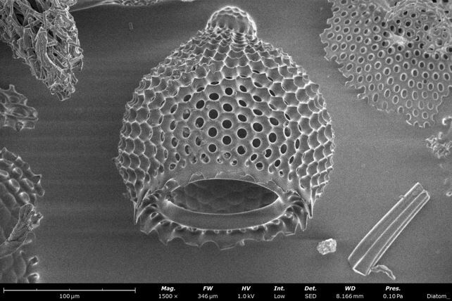
Select the Scanning Electron Microscope that meets your needs
25 Oct, 2021 | Newsletters

| It is a good time to be in the market for a scanning electron microscope (SEM) but where do you start? For researchers in academia or industrial R&D, it is important to match the SEM capabilities to the needs of the lab and its users. This webinar explains how different applications translate to requirements for different features and specifications on the SEM. In this webinar, we discuss what performance you can expect from a tungsten / FEG / in-lens FEG / UC FEG and how to deal with different types of samples (insulators, nanomaterials, sensitive materials). WATCH ON DEMAND Particle Analysis Applications using a Desktop SEM Phenom ParticleX Desktop SEM (Scanning Electron Microscope) is a multi-purpose desktop SEM designed for multiple applications such as Additive manufacturing, Technical cleanliness, Steel manufacturing, Batteries/ energy storage and Gunshot residue analysis. Beginning October 27, 2021, this six part series will focus on one particular analysis application and how the Phenom ParticleX Desktop SEM overcomes some of the most common challenges. Webinars will be made available to you for on-demand viewing shortly after the live sessions occur. |
| REGISTER NOW CALL US FOR A PERSONAL DEMONSTRATION Bookings are available now. Should you wish to use a desktop SEM or need further information, please contact our specialist team via email, enquiries@atascientific.com.au, or call us directly 02 9541 3500.  Take a closer look: Book your Phenom Pharos SEM demo The NEW Phenom Pharos G2 Desktop Field Emission Gun – Scanning Electron Microscope (FEG-SEM) has arrived and is ready for use at our office in Sydney. We invite you to send us your samples today! Limited time only. Phenom Pharos G2 combines all the capabilities of a floor-standing FEG-SEM in a tabletop system with the simplicity that Phenom desktop SEMs are known for. Fully integrated advanced detectors acquire high-quality images up to 2 million times in magnification, at 2.0 nm resolution and up to 20 kV. Users can also image soft, beam-sensitive or insulating samples at energy levels as low as 1 kV, obtaining high-resolution views into polymers and multilayer organic films without damaging or obscuring their nanoscale features. SEND US YOUR SAMPLES OR BOOK A COVID SAFE DEMO TODAY!! |
| Contact us for a demo Request a quote now Email us for more info |
 EXCITING ANNOUNCEMENTS: LATEST NEWS: WE ARE MOVING TO A NEW FACITIY!! To serve you better with more space. From 1 November 2021, we will be moving to our new state-of-the-art facility to expand and meet the growing demand for high-quality analytical instruments, service and support solutions. READ MORE HERE OUR YOUNG SCIENTIST ENCOURAGEMENT AWARD Aimed to provide young scientists with financial assistance to further their education and attend scientific meetings and conferences. For all our previous winners, CLICK HERE COVID-19 Customer Response Plan To help those that require analytical testing services adapted to the remote working environment. READ MORE HERE |


 02 9541 3500